Hardware
Parts choices
The parts our project needed were mostly known from the get‐go. We needed some kind of MCU, a display, an accelerometer, a battery, a GNSS and jelly bean voltage regulation + LiPo charging. There were a few parts we looked at optionally but they were all ruled out.
At the start we looked at using a GSM modem so the glasses could operate completely autonomously of a smartphone. The options we looked at were the Quectel M95, Quectel MC and Thales TX62 because these were in stock and reasonably priced. There’s a dev kit for Arduinos from Conrad but at 66+20 CHF the price was most of why we didn’t pick this one. The MC would’ve been ideal since it has a built‐in GNSS receiver, a programmable MCU and even BT. The problem is it operates only over 2G, which was discontinued in Switzerland. Lastly the TX supports LTE and the most power saving features but the only breakout we could find was Thales’, which was hideously expensive at €92 just for the carrier.
For the display, initially our group was split between using a transparent display or a regular opaque OLED. On the one hand, the transparent display would make the project’s aesthetic much better but at the same time there was little technical reason to opt for it in the first place. We found a suitable Parallax module for a 0.95” opaque OLED. Then the advantages of the opaque one were: higher availability, colour instead of the 1 bit transparent panel, lower cost. Of these colour was the most important feature because it means we could use good graphics. The only noticeable technical advantage of the Sparkfun transparent display was its 128x56 transparent bits instead of the ~96x found on opaque OLEDs. Ultimately our group had settled on trying out the transparent one and switching if we had second thoughts, but the transparent display was usable and we never looked back.
When we were initially selecting a microcontroller platform to use we were looking for something small and with BLE, and the STM32WB series caught our attention because they integrate all the RF circuitry on module and Paolo had already designed STM32‐carrying PCBs. However to use most of the IO requires a four‐layer PCB, and with the stm32 platform having a reputation for being more difficult to program for than chips with Arduino API support we changed our minds about the STM32. Part of what also influenced this choice was STM32s need to be programmed with ST’s own programmers and we’d need to look for or purchase these adding to the project cost. Upon Mr Koch’s suggestion we investigated using ESP32s and in hindsight that fit the bill much better. They’re simpler to program, have lots of flash space for large binaries, have almost complete flexibility in pin function mapping and we had dev kits available from the start.
The IMU and GNSS selection were certainly some of the simplest parts, what we had initially envisaged were a BMI160 and PA1616D respectively because these parts were available both in standalone SMD version from Digikey and on COTS breakouts from DFRobot and Adafruit respectively. The only requirements we had for these was that the IMU needed to be able to output interrupts. Meantime the GNSS had to have both an onboard patch antenna and the option to add an external one because we could screw up the external antenna in which case the internal one would be useful, while we were unsure the patch antenna would work if there was plastic covering it. At the end the parts we got were different to what was asked, although the MPU‐ 6050 worked fine and the Neo‐6M should’ve been adequate for our project.
Custom PCB
At the start we wanted to make the glasses’ electronics very compact because this would mean the electronics are easy to house and less bulky, the glasses could be made lighter, and this would be a good opportunity to improve PCB design skills. The desire to have a custom PCB is – alongside stock unavailability – much of what affected part choices at the start. At the start we thus made the following considerations:
| Advantages of custom PCBs | Disadvantages |
| Very simple enclosure design | High risk if there’s a showstopper design flaw |
| Lower cost of parts 4 | Layer boards are expensive |
| Much lower time for assembly because SMD pick and placing with a stencil is much faster than protoboard soldering. | More limited ability to repair parts after |
| Far more parts are available compared to THT. | Substantial lead time (~1 week + another for shipping) |
| Victor was interested in learning about this so good opportunity | A protoboard version would need to be developed anyway for testing |
| Less fragile | Signal probing requires test pads or headers that take up space |
Paolo designed the schematics and routing for a possible PCB design because it seemed like a sensible idea, but one of the important aspects we had forgotten until then was we could implement a sort of hybrid. Indeed, this was the solution we veered towards. By then Mr Koch had given us parts that were different to the initial proposal’s list, but with the PCB version it was trivial to implement compatibility with say both the opaque and transparent OLEDs. In hindsight, with the protoboard we gained very little in flexibility because desoldering and rearranging parts gets increasingly onerous. As an example, the Neo 6M GNSS couldn’t simply be swapped out for Paolo’s Adafruit module: the pinouts were different and resoldering wires differently would’ve taken considerable time.
Given our group wanted to ensure the PCB could work even if most of the SMD soldering failed, the PCB was designed to support any permutation of the following options:
- Display: NHD‐0.95‐9664G (opaque OLED) with custom driver, NHD‐0.95‐9664G on Parallax breakout, UG‐2856KLBAG01 (transparent OLED) with custom driver, UG‐2856KLBAG01 on Sparkfun breakout
- GNSS: PA1616D module (incl. external antenna connector and MOSFET for shutdown), Adafruit GPS V3 breakout
- IMU: MPU‐ 6050 breakout, BMI Since we wanted good flexibility the PCB was designed with 0 ‐ohm shunts on almost all lines with substantial risks, because then one could say bypass the MOSEFET in front of the GNSS in case there were a design flaw.
Much of the risk from a custom PCB was mitigated by Paolo simply using a dev kit ESP32 and using the COTS buck converter. This reduced the custom circuitry to the display driver, IMU, GNSS and buttons/LEDs. The dev kit ESP32 also meant a usable design was possible with just two layers, hence bringing down the cost as well. The dev kit also meant signal probing could be done with the ESP32’s pins, meaning this disadvantage was moot too.
Ultimately the reason we abandoned the custom PCB was the fact a protoboard would be necessary for testing anyways. Given the time needed for this even spending 2 ‐ 3 hours once parts and the PCB arrived for assembling a PCB and putting it in the reflow oven quickly became unjustifiable.
In retrospect, the schematics and PCB designed were flawless and compared to the final version would’ve only required some software tweaks to change the pins for the likes of SPI or i2c away from defaults. Besides pin mapping though a pared down version of the schematic and PCB design were what we settled with for the final protoboard. Since the PCB design has lots of 0 ‐ohm shunts for configuration or disabling faulty circuitry, assembly is also harder to get wrong compared to the protoboard, at least from Paolo’s experience with Xplore. Note: the schematics and PCB design are in separate documents.
Protoboard
Since we had to settle for the parts we already had and the custom PCB was not an option, we settled on assembling a protoboard with all our parts. The first step was simply placing all the components on the two boards and checking everything fit. Initially we’d underestimated the size of the buck converter for instance because we’d hoped it would fit horizontally. We also settled on keeping all components on the front, because the back side would be much more difficult to access while the protoboard is in the enclosure.
Luckily, unlike a PCB routing is not much of a problem because almost everything needs to be connected by wires to start with. To help, Paolo had stacking female 2.54 mm headers so wires could be soldered very securely by wrapping them too. The other advantage of these types of headers is they ease troubleshooting. This came in handy when Paolo had forgotten to solder the IMU’s interrupt line to one of the ESP32’s pins because one could connect a female‐female jumper between the headers. When interrupts weren’t working correctly on the ESP32 it was also easy to hook up an oscilloscope probe. With non‐stacking connectors the latter is still possible but very fiddly because the grabber falls off.
To connect the boards together Paolo tried a few solutions. The first idea was to use a generous dose of hot glue on each side since it’s one of the simpler things and it can glue basically anything. The problems are it comes off easily on a non‐porous surface like soldermask, and it’s too flexible. Hot glue would also become a hot mess if at any point in the future the hot air nozzle was necessary for any reason. The next idea was to use wire looping between holes on one board and the other so that when the wire is tight the boards would stay roughly firm. The problems with this are one wastes precious holes, the boards don’t stay perfectly rigid and the extra wires in the way would make it harder to follow signal and power wires added later. The current solution where the boards are simply soldered together with giant blobs of solder arose by accident because Paolo was bored and needed to melt a lot of solder to tin the iron. On normal PCBs this would be a poor way of attaching boards because the pads bear the brunt of the force and risk lifting. In this case being soldered on both sides and those pads having no electrical functionality means lifted pads aren’t a big deal.
Something useful when soldering the protoboard was to use enamelled wire for certain short sections. The advantage of this is it’s easier to cut and solder precisely because it’s single strand and one can burn enamel off in situ after part of the wire is soldered in place. This came in handy for the display board too, because we needed to solder to a very small pad where a regular wire wouldn’t work.
Protoboard Steps
The way Paolo roughly assembled it is as follows:
- Place the stacking headers and solder them in place, there’s 6 for the right board and two for the left
- Solder the buttons and their 3.3V pull‐up 10k resistors like in the image
- Align the left and right halves side by side as close as possible
- Melt a large blob of solder on the pads connecting the two boards
Considering the time to do this adding some no‐clean flux to the area is recommended
- Once the blob is hardened clean it with 99% IPA and q‐tips, even no‐clean flux should be cleaned off
- Repeat steps 4/5 for the other side
- Wire the 3v3 bus, ideally with red wire like in the image. You can use a section of protoboard like the very far right as a “hub” to connect everything to
- Wire the GND bus, like step 7
- Solder on the TP4056 charger remembering to put the necessary male pins. It’s normal the in+/‐ pins are in mid‐air, they’re not used since we use the type C plug instead.
- Connect positive and negative leads for the battery (red/black wires at very left), ideally use leads with a connector at the end. Here we’re using male pins.
- Add the slide switch where you find place. We’ve got the common connected to the GND bus and one of the positions is connected to the battery’s negative.
-
Make a resistor divider from the battery’s positive lead and feed the signal to the ESP32 on any of the ADC1 GPIOs (see here). A good spot for this is under the buck converter in the photo above.
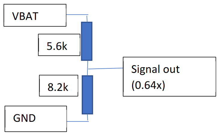
The reason for the resistor divider is the ESP32’s ADCs are only able to measure up to about 3.2 V. We wanted to avoid being right near the upper bound though so the ratio is \(\frac{8200}{5600+8200} \approx 0.64\) because this allows us to feed up to 5V. In a second stage such a voltage could be helpful if one needed to monitor USB bus voltage as though it were VBAT. Precision of measurement wasn’t a big deal so using only 2.24 (battery at 3.5V)‐2.69 (battery at 4.2V) V as the ADC input is perfectly fine for us.
- Solder on the buck converter to the board, making sure to connect its in+ to the tp4056’s
out+.
Do not connect in+ straight from the battery because this bypasses the charging board’s protection circuitry to prevent nasty stuff like over discharge protection.
- Making sure no IMU/GNSS/ESP32 etc are plugged in, supply ~4.2 V from a current‐limited (ideally set to ~50 mA) lab supply to the leads that would usually connect to the battery. Trim the trimmer so the 3v3 bus is as close as possible to 3.3 V. Sweep the lab supply down to about 3.3 V and make sure the 3v3 bus stays close to 3.3 V. Close means it should really be 3.1‐3.5 or thereabouts. Remember the trimmer is a multiturn one in any case. Power down the lab supply.
- Put a small dollop of hot glue on the trimmer to ensure it doesn’t get knocked and to deter others from tampering with it for fun.
- Repeat the lab supply sweep to check gluing didn’t move the trimmer either.
- Add 10k i2c 3v3 pull up resistors for the IMU
- Hook up the IMU’s signal pins to the ESP32. SDA -> 21, SCL -> 22, INT -> 32 Since these are stacking connectors the easiest is to strip insulation from wire, tin the wire very lightly, wrap the tinned wire around a given pin and only then apply solder. To connect the IMU, make sure to solder on right angle wires obviously.
- Hook up the 3 left‐most pins on the top of the right board and the 3 left‐most pins on the bottom of the right board to: 3v3, GND, MOSI (ESP32 pin 23), DC (ESP32 pin 19), CLK (ESP pin 18), CS (ESP32 pin 5). On the header it doesn’t matter what wire goes where because this connects via jumper wires anyways. Just make sure to hook everything up right when going there.
-
Cut all jumpers on the display board, solder on male right angle headers and for some reason we also needed enamelled wire because some soldered pins were not connected.
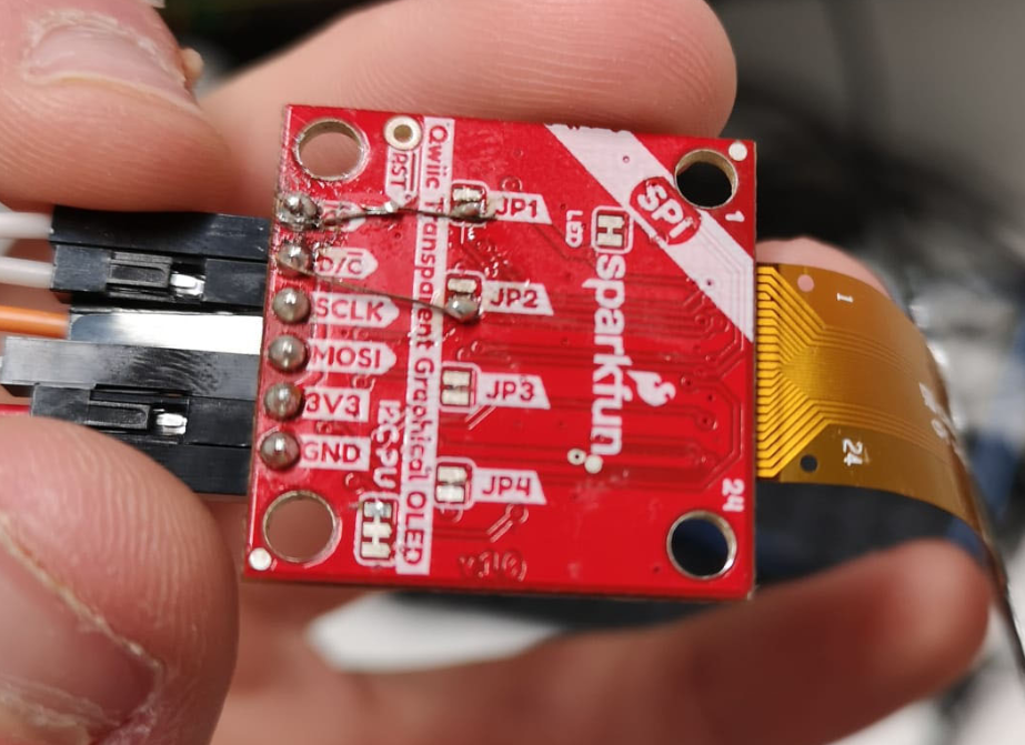
-
Plop in the ESP32 with the micro‐B socket facing towards the right
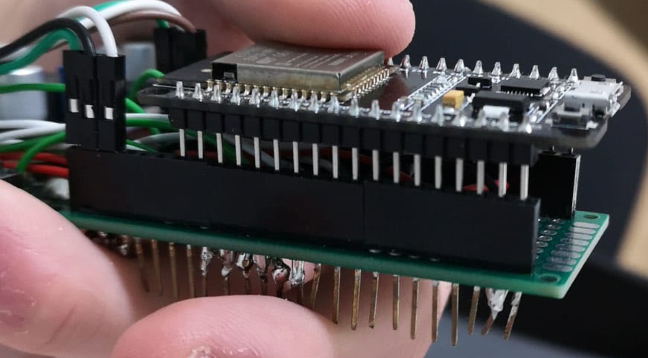
- Although we didn’t wind up using the GNSS, you can hook up the RX/TX pins on there to pins 16/17 if you have a module that does work.
GNSS
We wanted to integrate a GNSS module on the glasses. The idea is so the glasses could pick up their own position. What we wanted to do at the start was to let the glasses get their start location, send this to the phone, the phone would collect all the directions from Google’s directions API and then send them all to the ESP32 in one go. Then the ESP32 listens to the GNSS, and the next direction is shown when the onboard GNSS reports the glasses are at the right place. The advantage of this system is the glasses could be used somewhat standalone and offline after setting the desired directions. At the start Paolo was testing with TinyGPSPlus and his own Adafruit GPS Module and these worked well. However when we tried using a Neo‐6M module in the same way nothing was coming through on the serial line and it seemed strange. Importantly, any normal DIY‐intended GNSS spits out data over UART in a standard NMEA format so the interface is drop‐in compatible. After trying another module and meantime finding others had success with our module, an ESP and TinyGPS++ we found on close inspection the ublox module was misaligned during placing so the RX/TX pins were shorted. To identify this the easiest is to have a look at the datasheet and make a list of the pins one knows are supposed to be connected. In this case we found the following list, and after measuring continuity there were shorted pins fixed as described in the video.
- 3: Timepulse (aka PPS)
- 8/9: VCC_RF for the external antenna
- 10, 12, 13, 24: GND
- 11: RF_IN for the external antenna
- 20: Tx
- 21: Rx
- 22: V_BCKP from coin cell
- 23: VCC
IMU
To implement the falling granny feature, it was quick to tell we needed an accelerometer so we could detect rapid movements. The MPU 6050 is one of the most common IMUs, and that proved very helpful in our project. At the start Paolo used Adafruit’s MPU 6050 library, and it was very straightforward to get a small Arduino sketch running which could print out current acceleration and gyroscope info. However polling the IMU like this would wind up wasting considerable ESP32 time and energy, so we needed to switch to interrupts. The advantage of these is once the device is configured correctly it will autonomously sample the accelerometer and trigger the ESP32 when there is a granny fall event. This means it’s less likely to have false negatives too because with polling one can only sample the accelerometer so often while internally the IMU samples the accelerometer at 200 Hz. At the start of the project we had done some research on the IMU and found that with the stock DMP firmware it could output interrupts for the following (along with housekeeping like FIFO full and such):
- Free fall
- Motion detected
- Zero motion detected – basically used for checking inactivity
One could also trigger other interrupts if one had access to documentation for programming the IMU’s DMP. It’s a sort of small processor that’s user programmable and one of the main features behind the MPU’s popularity. Unfortunately, from what we’d found online the documentation is no longer publicly accessible. This limited what we could do with the IMU to just the aforementioned events. On top of this though, while trying to use the Adafruit library it became very clear it had some issues on ESP‐IDF and the Adafruit library turns out to be a simple wrapper for the i2cdevlib library which has a version with native ESP32 support. After switching libraries, Paolo adapted an example to pick up freefall, motion and zero motion interrupts but still using the Arduino IDE.
The main hurdle with getting i2cdevlib working is the accelerometer needed to be calibrated, and the thresholds for events tuned. For this, calibration was done with a post here and the MPU6050_raw example from the library, after which thresholds were determined by doing a binary search for thresholds that would trigger with a balance of false readings. Note the calibration values are obviously device‐specific, so if one wanted to scale the code one would need a calibration program to write values to flash with less trial and error than doing everything by hand. The main thing we found is the freefall detection has too many false negatives to be usable, and the motion detection worked well exactly for freefall detection. The ideal would be to use the gyroscope so one only triggers when the glasses fall downwards, but for the IMU to autonomously output an interrupt for this, one needs to make a program for the DMP which faces the documentation problem. In any case, at the moment the user would have to throw the glasses quite hard for horizontal detection to trigger fall detection anyway, so we settled for motion detection which checks for any axis having high acceleration. Importantly, to do any of these interrupts one needs to read the datasheet but for some reason Invensense cut out specifications for the interrupts we want to use in the later versions. To get the full specifications one needs to look at revision 3.1 under section 8.
Given we had to get through the datasheet anyways we also thought to look at power management. Originally power management was a completely optional feature, but it turns out at this point it was worth handling at least the IMU’s power management. So we came up with the following FSM for the system:
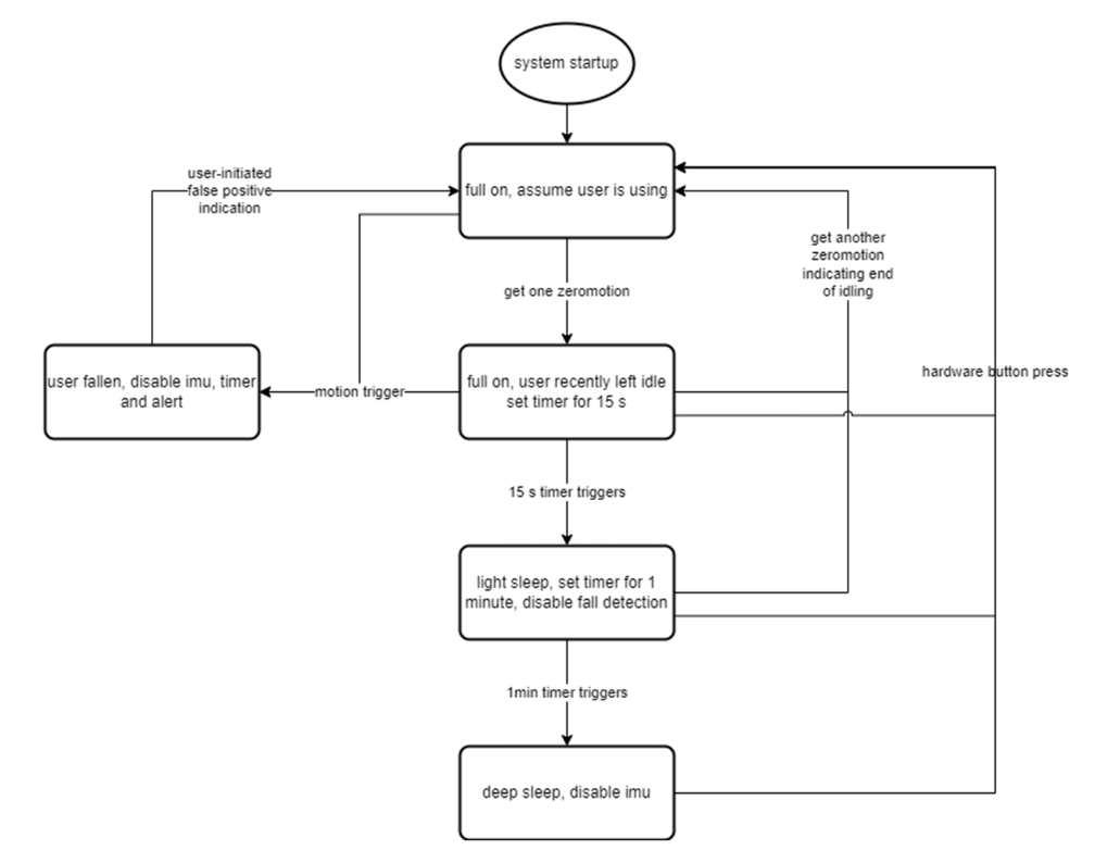
In particular, we took advantage of the zero‐motion interrupt to set the IMU to sleep or wake up when it’s left to idle for a bit or when it’s picked up. The zero motion is tricky to tune, because one needs to prevent the IMU from waking up spuriously while also setting the zero‐motion threshold low enough that the glasses don’t require constant shaking to stay awake. Unfortunately the device only has one threshold (set with setZeroMotionThreshold) for this, so there are quite a few false positives both ways. The other major issue is the zero‐motion interrupt can only be set to trigger after no more than 16 seconds (first zeromotion) because the 8 bit register has an LSB of 64 ms. This is why there’s a second full on state that starts a timer. 15 s is just an example, for a production version this would probably be user configured or pre‐set to about 5 minutes.
By this point, the IMU was working well but through the Arduino IDE and its associated API, both of which run surprisingly differently to ESP‐IDF and the native ESP32 API. The two main differences are the Arduino IDE makes several defines and the sdkconfig file configuring the device is not straightforward to modify. At the start we tried integrating the esp32‐native version of i2cdevlib’s MPU6050 component, and basics like reading accelerometer values were mostly trouble‐free. However, the serial console was clearly corrupted shortly after startup. To troubleshoot this, first Paolo tried temporarily cutting out the rest of the project and then used a new stock ESP‐IDF project. With a new project everything worked (see “Finding SPI pins”).
Troubleshooting
Fixing a GNSS Module
See here
Finding SPI pins
At the start of the project none of us had worked with the ESP32 platform before so we had some problems understanding say what VSPI vs HSPI meant. Since we just wanted the simplest everything‐default configuration it was faster to simply probe the pins with an oscilloscope because Sparkfun’s guide only showed their Qwiic connections and not pin numbers, and they were using slower i2c. Importantly, since these are rather fast digital signals using grabbers is helpful to maintain one’s sanity. With the ESP32 running an example display sketch and after finding the right pins we got this:
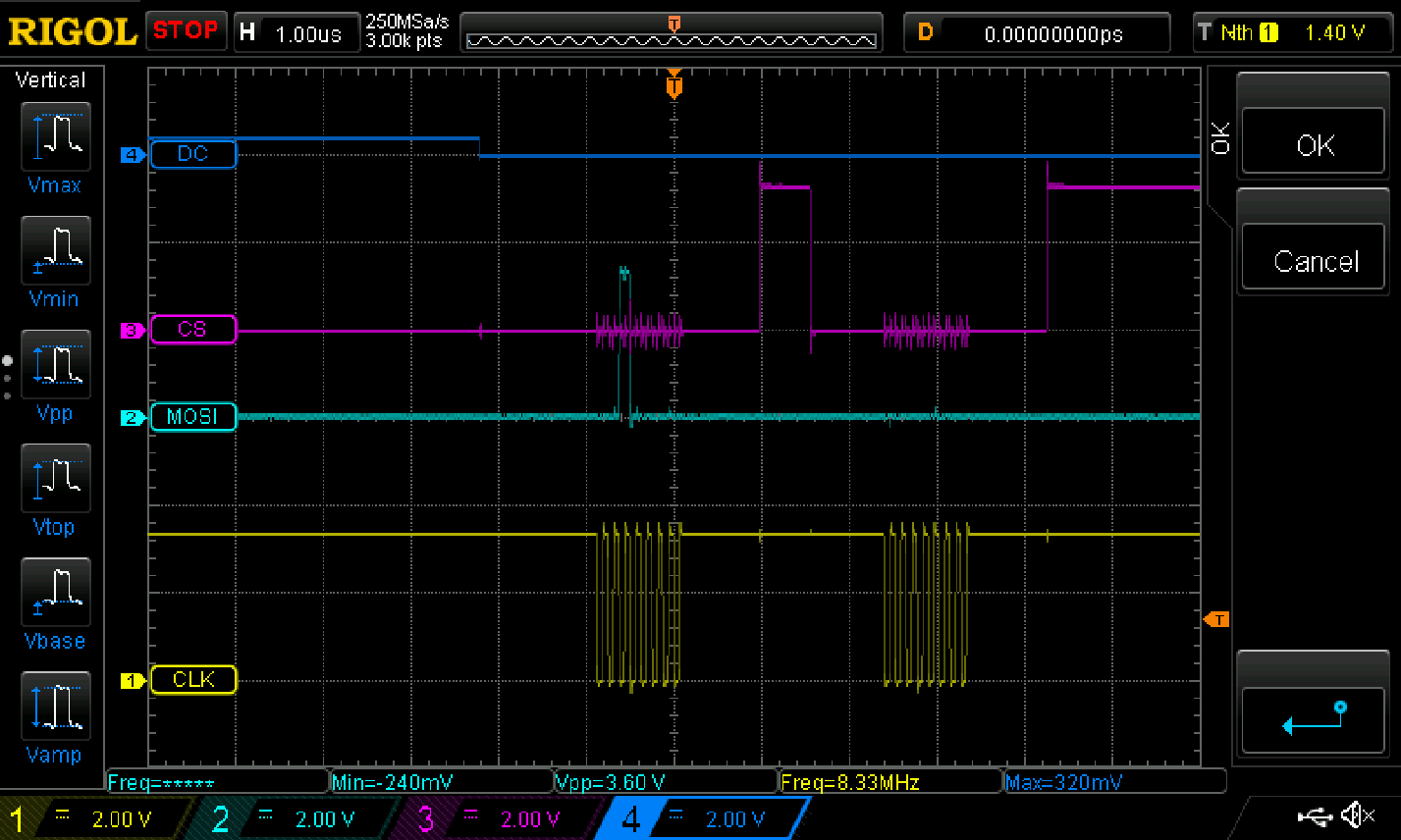
To figure out which signal was which to start with, the easiest is to start with the clock because one knows that during transmissions this runs at several MHz. One can set up an nth‐edge trigger if one wants to prevent noise triggering capture. In this case it’s the 8 th rising edge because 8 eight clock cycles are needed per byte transferred. This yields the clock pin at 8 MHz on pin 18 and MOSI on 23 by default, and DC/CS are 19/5 but these are entirely picked by us.
Diagnosing garbled serial console
The reason for the corrupted serial console line turns out to be that we had enabled the power management API to do things like dynamic frequency scaling for us to avoid running at the higher 160 MHz. Unfortunately, it appears the feature also garbles output because the UART driver clock source is switched from the APB clock to the REF_TICK clock that runs at 1 MHz.
For a normal 115200 baudrate the REF_TICK the UART is driven by doesn’t divide by 115200, hence the timing is always very off. In this case the simplest solution was to simply disable dynamic frequency scaling because higher baudrate output was more important to us, in another case reducing the baudrate helps a lot because an imperfect clock division is less of an issue. The UART receiver samples the data at its preconfigured baudrate as described here, so any significant deviation from this causes garbled data but much less at lower baudrates. At 115200 bps and 1 MHz base clock the divisor would need to be 8.68 while at 9600 bps it’s 104.17. Assuming the hardware rounds down, the integer divisors are 8% and 0.1% below the desired respectively. When dynamic frequency scaling is disabled, the UART is sourced from the APB clock at 80 MHz and the divisor for 115200 bps is then 694.44, so 694 is only 0.6 ‰ below and UART in normal operation has no visible corruption.